4- stages Project Scheme's:
The Project was divided into 4 stages as shown below:
The Project was divided into 4 stages as shown below:
----------------------------------------------------------------------------------------------------
Power Electronics Stage Calculation and Simulation
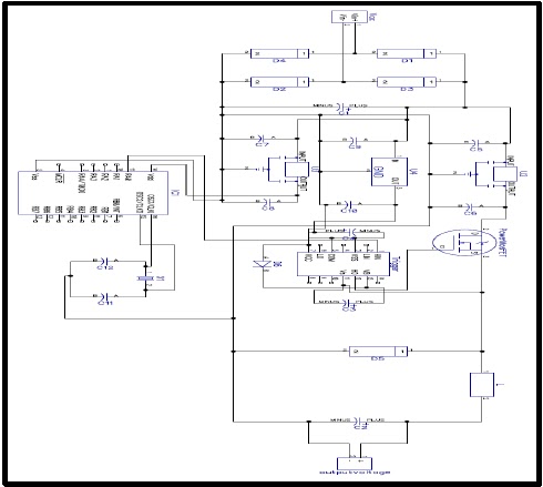
The circuit contains a Bridge Rectifier, Buck-Boost DC-to-DC Convertor, and after all the calculation was done to find the suitable components values for the Buck-Boost DC-to-DC Convertor Or-Cad software was used to simulate the Electronic circuit as shown below:
The output voltage from the bridge rectifier circuit shown below:
----------------------------------------------------------------------------------------------------
Project Implementation:1- 4 Schottky diodes
2- Capacitors, each 1000uF
1: MOSFET (IRLB3036)
2: Schottky diode
3:Capacitor of 68uF
4:Inductor of 68uH
----------------------------------------------------------------------------------------------------
Full wave bridge rectifier with RC circuit output
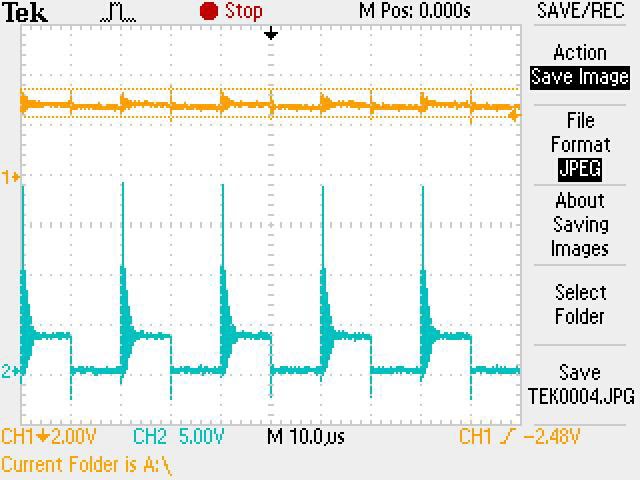
Buck-boost converter output after twisting wires and shorten them
1. An oscillator of 8M and a 1KΩ were connected to a PIC16F84A microcontroller.
2. A 7812 regulator was connected to the driver chip.
3. A 7805 regulator was connected to the PIC16F84A microcontroller.
4. A 7805 regulator was connected to the buck-boost circuit.
5. A diode and a zener diode were connected in series to the MOSFET of the buck-boost converter to reduce the transient of the converter's output.
The schematic diagram for the electronic circuit using Dip Trace
The BCP Layout for the electronic circuit
| Top Layer | Bottom Layer |


